
BUILT FOR PRECISION
Semiconductor
done with care.
Process-aware maintenance for fab-adjacent and microelectronics environments. Our team works with each customer to understand restrictions, materials, documentation, and the most effective service schedule.
Discuss this service ↗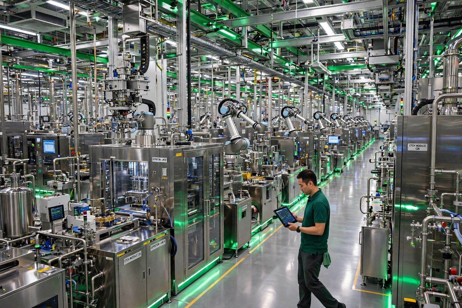
FLAWLESS / SEMICONDUCTOR
OUR SCOPING PROCESS
Every detail
has a purpose.
01
Restricted-zone handling and particulate-control considerations
Confirmed as part of a facility-specific proposal.
02
Approved process-area materials and cleaning sequences
Confirmed as part of a facility-specific proposal.
03
Coordination with maintenance and facility operating windows
Confirmed as part of a facility-specific proposal.
Cleaning is tailored to your facility’s written requirements; we do not promise semiconductor yield improvements or ISO certification.
START WITH A SMARTER SCOPE